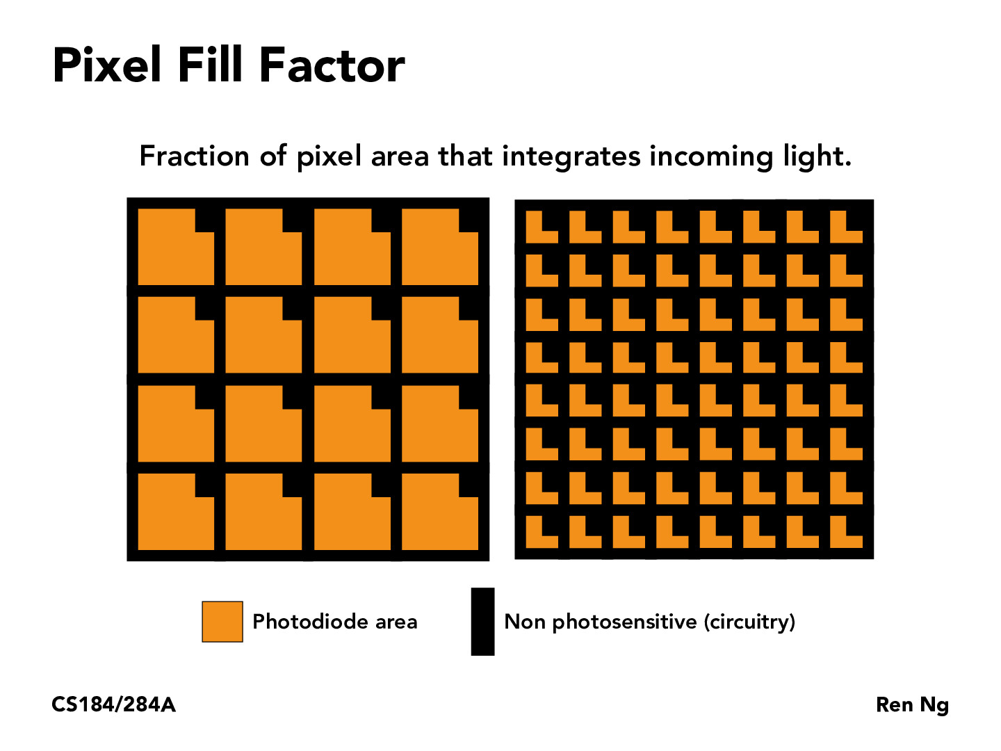
Is there a reason that the per-pixel circuitry needs to be on the corner of the pixel? Is there a reason it couldn't be put behind the photodiode? Does this effect get fixed anyways due to the microlenses?
jenzou
frankieeder: Slide 17 has a diagram of the circuitry of the active pixel sensor photodiode: https://cs184.eecs.berkeley.edu/sp19/lecture/21-17/image-sensors Beneath the photodiode is the potential well. It seems that the circuitry would need to be at the same level as the photodiode?
amandaawan
This is interesting - with an increase in the number of pixels in a screen, the pixel fill factor will decrease... It seems that there is a tradeoff between the total amount of electrons "detected" to be part of the bucket vs the number of pixels on the screen. Does this mean that we would theoretically need to increase the exposure in the second image vs the first image to get the same amount of brightness?
Is there a reason that the per-pixel circuitry needs to be on the corner of the pixel? Is there a reason it couldn't be put behind the photodiode? Does this effect get fixed anyways due to the microlenses?
frankieeder: Slide 17 has a diagram of the circuitry of the active pixel sensor photodiode: https://cs184.eecs.berkeley.edu/sp19/lecture/21-17/image-sensors Beneath the photodiode is the potential well. It seems that the circuitry would need to be at the same level as the photodiode?
This is interesting - with an increase in the number of pixels in a screen, the pixel fill factor will decrease... It seems that there is a tradeoff between the total amount of electrons "detected" to be part of the bucket vs the number of pixels on the screen. Does this mean that we would theoretically need to increase the exposure in the second image vs the first image to get the same amount of brightness?